
Driving waveforms
Having the electrical connections figured out, there is the problem of what kind of signals to feed into the display panel. In theory, it is simple enough: just shift in some bits to the source driver register and step the gate driver register. In practise, however, there are a few gotchas..
At first I had some trouble getting anything to happen. It turned out to be a combination of badly connected cables, wrongly defined pinouts and various bugs. However, the first thing I did manage to get to display is this brute force pattern generated by dumping rand() output into the GPIO pins:
That seems to be a good way of checking that all signals are connected and all voltages are ok.
Gate driver
The gate driver is definitely the easier one. Its purpose is to simply select one row of the panel for updating. How this is done is that you shift in a single "1" bit, and then "0" bits every time you want to advance to the next row. The "1" bit will shift through the register until it falls off the far end.
What's funny, though, is that you can actually see this happening:
That video shows the active row driver line visible at the edge of the panel. Apparently the electrophoretic material extends a bit past the actual display area, so that anything that happens in the electrodes underneath becomes visible.
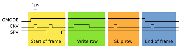 Gate driver waveforms.
Basically, to start a frame, you toggle GMODE (gate output enable) high and activate SPV (start pulse vertical, active low) for one CKV clock cycle. After that you toggle CKV for each row you want to advance. It seems that the gate driver is only on while the CKV is high, and also that the on-off ratio of CKV is important. It seems necessary to have CKV off much longer than it is on, otherwise the image leaks to other rows also. Probably some kind of residual charge which must be allowed to dissipate.
The following table lists the timings that I have found suitable for my panel:
| Purpose | CKV high time | CKV low time |
|---|---|---|
| Frame start/end pulses | 1 µs | 4 µs |
| Write data onto row | 5 µs | 200 µs |
| Skip row without writing | 1 µs | 100 µs |
| Bulk clear | 20 µs | 200 µs |
Source driver
The source driver is not very complex either. You shift in 800 pixels of data, 2 bits per pixel. After all the data is in the shift register, you pulse the latch enable to store it into the latch. Then you pulse the output enable when you want to write out the row.
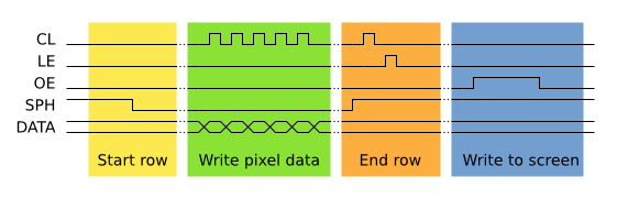 Source driver waveforms.
The SPH signal starts the row register, and should remain low for the duration of the row. Pixel data is shifted in 8 bits at a time, so that each byte contains information for 4 pixels. Therefore, a total of 200 pulses on CL clock signal. After the row has been shifted in, the LE (latch enable) signal is pulsed high to load the data into the output latch. Finally, to write the row, the OE signal should be raised simultaneously with the gate driver CKV signal.
This much was easy enough to guess based on the public information. However, doing just that, nothing happened. One crucial piece of information is still missing: the meaning of the 2 bits that define the state of each pixel:
| Bit 1 | Bit 0 | Action |
|---|---|---|
| 0 | 0 | No action |
| 0 | 1 | Draw black |
| 1 | 0 | Draw white |
| 1 | 1 | No action |
And guess who was using 0x00 0xFF as test pattern..
Conclusion
These waveforms are enough to get basic images onto the E-Ink panel. In reality the subject is a lot more complex: there are all kinds of temperature dependencies and various ways how to switch pixels as quickly and accurately as possible. In fact, when you buy through the official channels instead of eBay, the panel manufacturer will provide a waveform file which contains all of the timings in some proprietary format.
Update: Apparently there are several different versions of the ED060SC4 display. If you have one with all wires present on the connector, see sprite_tm's findings about the differences.
– Petteri Aimonen on 11.6.2013